
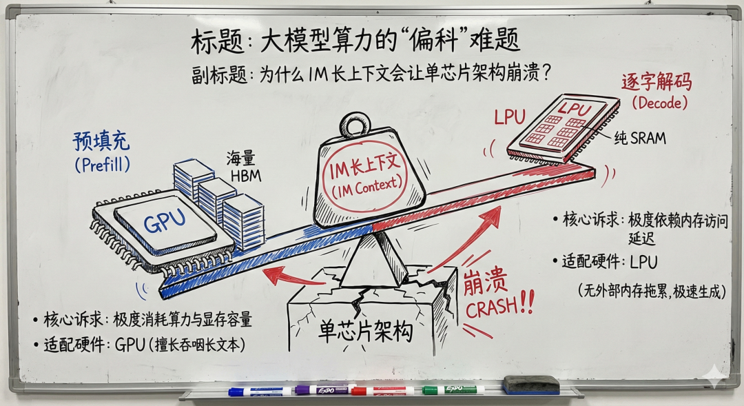
When handling ultra-long contexts of 100K or even 1M tokens, AI compute runs into an obvious lopsidedness:
- The prefill stage, which processes the input, burns enormous floating point compute and memory capacity
- The decode stage, which generates the output, depends on extremely low memory latency
No single architecture today handles both of these well.
1. PD Disaggregation: Let Each Chip Do What It Is Good At
Since there is no perfect single chip, architecture has to make up for it. The industry is shifting toward heterogeneous cooperation across hardware:
- Heavy compute for heavy computation: let GPU arrays with vast amounts of high bandwidth memory (HBM) handle long text in batches and produce tens of GB of KV cache
- Fast cache for generation latency: hand the decode work that follows to Groq's LPU, which drops off-chip memory in favor of pure SRAM and emits tokens one at a time at nanosecond latency
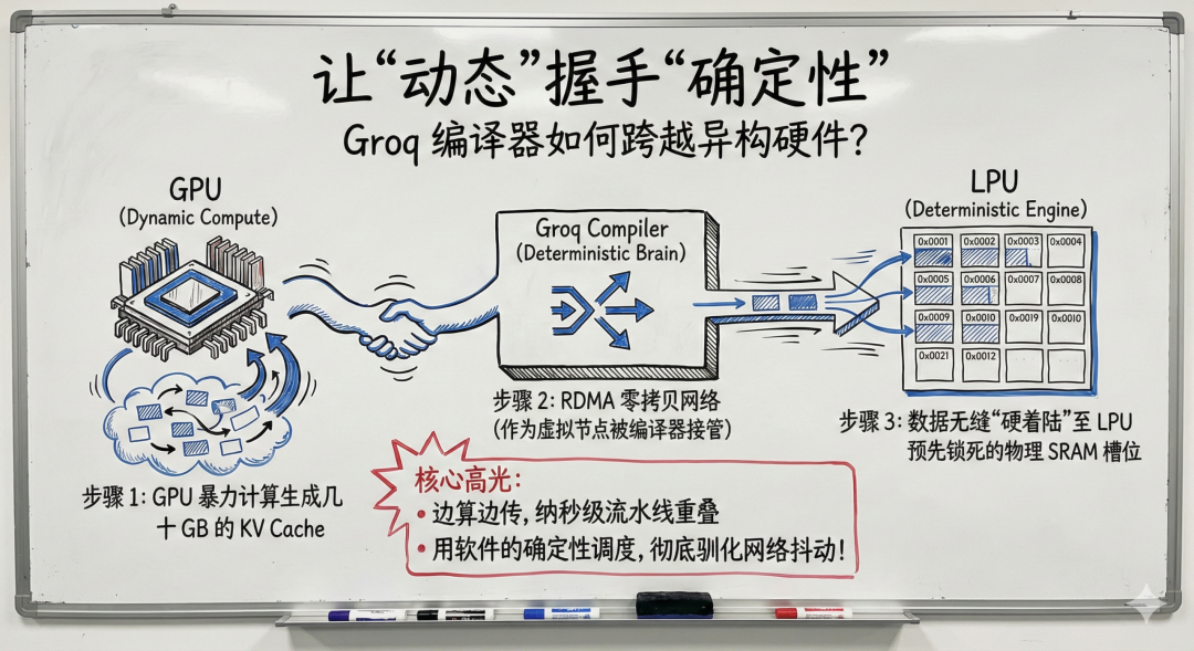
2. The Compiler: Taming a Dynamic Network With Determinism
Joining a GPU to an LPU takes more than running a network cable. GPU computation is dynamic, while the LPU needs absolutely precise cycle alignment. Control the inflow of data badly and the LPU's tiny SRAM overflows.
The key here is extending the compiler's view of the topology. Groq's compiler treats the physical NIC as a virtual node with a known latency, and through static memory allocation and RDMA zero copy, data produced on the GPU side passes straight through the network and lands in physical SRAM slots the LPU locked in advance. Transfer runs alongside computation, and with nanosecond-scale pipeline overlap and FIFO queues at the edge, network jitter that cannot be controlled from outside becomes a deterministic data flow that can be controlled from inside.
3. CoPoS Panel-Level Packaging Backed by TGV
Software optimization only solves the problem at the transport layer. CoPoS panel-level packaging backed by TGV (through glass vias) eliminates the distance problem at the physical level.
Past the Wafer Size Limit
Traditional silicon-based CoWoS packaging is bounded by the physical edge of a 12-inch round wafer. CoPoS replaces the silicon with large rectangular glass panels of 500mm and up. GPU chiplets, LPU chiplets, HBM and SRAM can all be packed at high density inside the same module. A heterogeneous system that used to require rack-level deployment shrinks onto a single substrate.
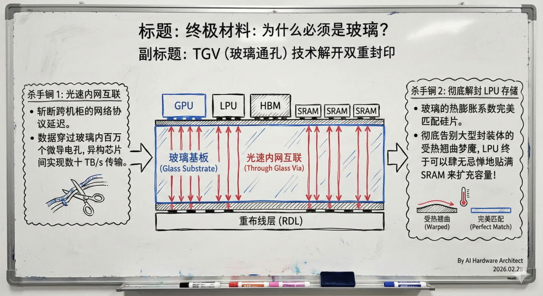
Interconnect Bandwidth and Memory Expansion
The dielectric properties of a glass substrate, together with millions of TGV microvias inside it, eliminate the network protocol latency of transfers between devices. Data movement bandwidth between GPU and LPU can reach tens of TB/s. More importantly, the thermal expansion coefficients of glass and silicon match, so the inside of an LPU package can be covered with SRAM memory chiplets to expand capacity without failing from thermal warping.
Summary
The future of large model inference hardware is more than a stack of advanced process nodes. A compiler spanning heterogeneous architectures as the software brain, paired with the physical skeleton of glass substrates and advanced packaging, achieving high throughput and low latency together on a single panel: that direction is getting close to reality.